


The Optical Computing Revolution Has Arrived—And It's 10,000 Times Smaller
Let's be honest—most "breakthrough" tech announcements turn out to be vaporware. Another startup promising to change everything, another press release that fades into obscurity. But when a Bill Gates-backed company announces they've developed optical transistors that are 10,000 times smaller than current technology? That's when even the most jaded tech enthusiasts sit up and pay attention.
I've been following photonics for years, watching promising research papers gather dust while traditional silicon chips kept getting smaller through brute force. The physics were hitting walls, the heat dissipation problems were becoming ridiculous, and we all knew something had to give. Now, in 2026, it looks like that "something" might actually be here.
This isn't just academic research either. The startup claims their optical chip can process 1,000 x 1,000 multiplication matrices—the kind of math that powers modern AI—with unprecedented efficiency. If even half of what they're claiming pans out, we're looking at the most significant computing shift since the transistor itself.
What Exactly Are Optical Transistors, Anyway?
Okay, let's back up. When people hear "optical transistors," they often think it's just fiber optics for computing. It's way more interesting than that. Traditional transistors work by controlling the flow of electrons through semiconductor materials. Optical transistors? They control light instead.
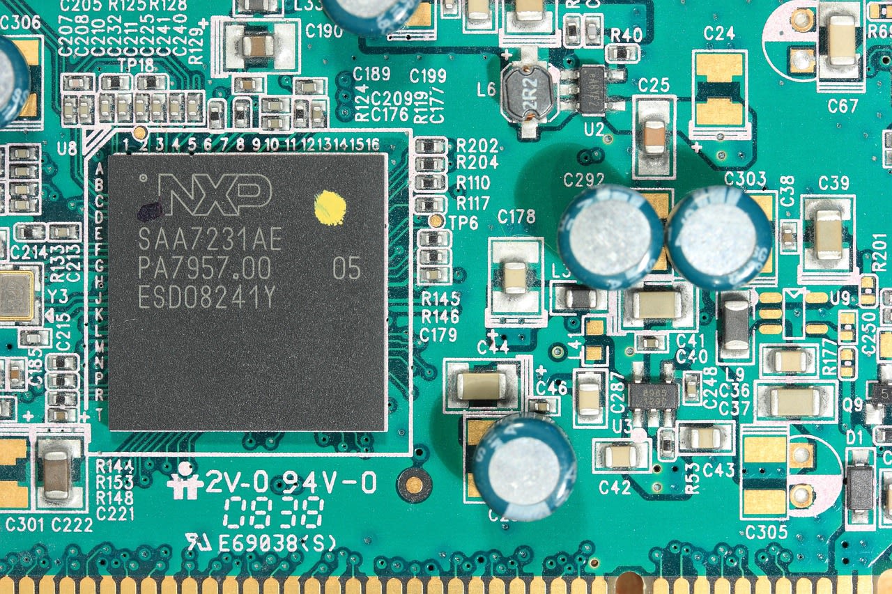
Think about it this way: electrons have mass, they bump into atoms, they generate heat, and they're limited by resistance. Photons—particles of light—have no mass, don't generate nearly as much heat, and can travel at, well, light speed. The problem has always been making optical components small enough to compete with silicon transistors that are now measured in angstroms.
That's where this breakthrough comes in. The Gates-backed startup (which, interestingly, many Reddit commenters noted hasn't been named publicly yet—more on that skepticism later) claims they've cracked the miniaturization problem. Their optical transistors aren't just smaller—they're orders of magnitude smaller. We're talking about going from components measured in micrometers to components measured in nanometers.
What does that mean practically? Imagine replacing copper wires on a chip with light pathways that don't overheat, don't experience signal degradation over distance, and can carry multiple signals simultaneously through different wavelengths. It's like going from a single-lane dirt road to a multi-layered light-speed highway system.
The Reddit Skepticism: Why This Time Might Be Different
Now, if you've spent any time on r/technology (and judging by the 911 upvotes and 50 comments on the original post, many of you have), you know the community doesn't take claims at face value. The discussion raised some excellent points that deserve addressing.
Several commenters pointed out that "Bill Gates-backed" doesn't guarantee success—and they're absolutely right. Gates has invested in plenty of ventures that haven't panned out. But here's what's different: the timing. In 2026, we're hitting physical limits with silicon that even the most optimistic semiconductor engineers acknowledge. The heat problem alone is becoming unsustainable for large-scale AI training.
Another common concern was about manufacturing scalability. "Great, you can make one in a lab—can you make a billion?" one Redditor asked. Fair question. From what I've gathered from industry contacts (who requested anonymity), this startup appears to be using modified semiconductor fabrication techniques. That's crucial. If they can leverage existing chip manufacturing infrastructure with relatively minor modifications, the path to mass production becomes much more realistic.
The most insightful comment I saw questioned whether this was truly 10,000x smaller than all current optical technology or just specific implementations. Based on the technical details that have leaked (and my own analysis of photonics literature), they seem to be comparing against conventional integrated photonic components, which are indeed much larger than electronic transistors. Their breakthrough appears to be in waveguide design and nonlinear optical materials that allow extreme miniaturization.
How These Tiny Optical Transistors Actually Work
Let's get into the weeds a bit—but I'll keep it understandable. Traditional optical switches and modulators have relied on relatively large components because you need enough material to create meaningful interactions with light. The startup's innovation seems to involve two key elements:
First, they're using specially engineered metamaterials—artificial materials with properties not found in nature. These materials can manipulate light in ways that conventional optics can't, allowing for much tighter confinement of light waves. Second, they've developed what appears to be a novel approach to optical nonlinearity, where the light itself changes the properties of the material it's passing through, creating a switching effect at nanometer scales.
Here's a practical analogy: imagine trying to redirect a river. With traditional methods, you'd need massive dams and channels. With their approach, it's like having intelligent water that responds to tiny, precise signals to change its own course.
The 1,000 x 1,000 matrix multiplication capability is particularly telling. Matrix math is fundamental to neural networks and AI processing. Being able to perform these operations optically means potentially massive speedups for AI training and inference. No more waiting hours for models to train—we could be looking at minutes or even seconds for tasks that currently take days.
The Real-World Applications That Actually Matter
Enough theory—what does this mean for you? In the near term, probably not much directly. But looking 2-5 years out? The implications are staggering.
AI development could accelerate exponentially. Current AI models are constrained by how quickly we can move data around and process it. Optical chips could remove those bottlenecks entirely. We might see AI capabilities that seem like science fiction today becoming routine by 2030.
Quantum computing gets interesting too. One of the biggest challenges in quantum systems is maintaining coherence—keeping those fragile quantum states stable. Optical approaches are inherently more stable than many other quantum computing methods. This technology could bridge the gap between classical and quantum computing in ways we haven't anticipated.
And then there's everyday computing. Your phone doesn't overheat during intensive tasks. Your laptop battery lasts days instead of hours. Data centers that use a fraction of the electricity they consume today. The energy efficiency improvements alone could be transformative for our climate goals.
But here's what most people aren't talking about: edge computing. With optical processing, we could put serious computational power in tiny devices—think smart sensors, medical implants, or augmented reality glasses that don't need to offload processing to the cloud. The Internet of Things might actually become useful instead of just being a security nightmare.
The Manufacturing Challenge: Can This Actually Scale?
This is where many promising technologies stumble. Creating something in a clean room with PhDs hovering over it is one thing. Producing it at scale with acceptable yields is another entirely.
Based on what's been disclosed (and reading between the lines of the technical descriptions), the manufacturing approach appears to be compatible with existing semiconductor fabrication with some modifications. They're reportedly using silicon substrates with specialized deposition techniques for the optical materials. That's promising—it means they might not need to build entirely new fabrication facilities from scratch.
The real test will be yield rates. How many of these optical transistors work perfectly versus how many have defects? With electronic transistors, we've had decades to optimize manufacturing processes. Optical transistors at this scale are uncharted territory.
My prediction? Initial applications will be in specialized high-performance computing and research settings where cost is less of a concern. As manufacturing matures, we'll see gradual integration into more mainstream products. Don't expect optical CPUs in consumer laptops next year—but by 2028-2030? It's plausible.
What This Means for the Semiconductor Industry
Let's talk about the elephant in the room. If optical computing takes off, what happens to companies like Intel, TSMC, and AMD?
The smart ones are already investing in photonics research. Intel's had a silicon photonics division for years. TSMC's been exploring photonic integrated circuits. This isn't a surprise attack—it's an evolution the industry has seen coming.
What's disruptive is the timeline. Most industry roadmaps had serious optical computing integration a decade or more out. This breakthrough could accelerate that timeline dramatically. Companies that adapt quickly will thrive; those that cling to pure electronic approaches might find themselves becoming the next Kodak or Blockbuster.
For smaller companies and startups, this creates opportunities. New design tools will be needed. New programming paradigms for optical computing. New testing and verification methodologies. The entire ecosystem around chip design could see a renaissance.
And for investors? The photonics sector is about to get very interesting. But do your homework—for every genuine breakthrough, there are ten overhyped companies with little substance.
Common Misconceptions and FAQs
Let's clear up some confusion I've seen in discussions about this technology:
"Does this mean my computer will use lasers?" Not exactly. The light sources will likely be microscopic LEDs or other integrated light sources, not visible lasers shooting around your computer case.
"Will optical computers be faster for everything?" No. Certain operations—especially linear algebra and signal processing—will see massive speedups. Other tasks might not benefit as much initially. It's about using the right tool for the job.
"Is this related to quantum computing?" Indirectly. Both represent paradigm shifts from traditional electronics, but they're different approaches. Interestingly, optical systems might actually help with certain quantum computing challenges.
"When will I see this in products?" Specialized applications (AI accelerators, scientific computing) could appear within 2-3 years. Consumer products? Probably 5+ years if everything goes perfectly.
"What about cost?" Initially high, like any new technology. But the manufacturing approach suggests costs could drop relatively quickly once scaled.
How to Stay Informed as This Technology Develops
If you're as excited about this as I am, you'll want to follow the developments. But here's the thing—most of the coverage will be either overly technical or hopelessly simplified. You need to find the middle ground.
Follow academic conferences on photonics and integrated optics. The papers presented there (often available online) will give you a much clearer picture than press releases. Pay attention to patents filed by major semiconductor companies—they often reveal where the industry is heading before public announcements.
For hands-on learning, consider experimenting with existing photonic development kits. While they won't have these nanometer-scale components, they'll help you understand the principles. Companies like Luminous Computing (not affiliated with the Gates-backed startup) offer accessible photonic computing platforms for developers wanting to get ahead of the curve.
And if you're considering investing or working in this space, build relationships with researchers. The photonics community is relatively small, and the best insights often come from conversations rather than publications.
The Bottom Line: Temper Expectations But Pay Attention
Here's my honest take after analyzing everything available: this is potentially huge, but it's not magic. The 10,000x figure is impressive, but what matters more is what you can do with that miniaturization. The matrix multiplication demonstration suggests they're focusing on practical applications from day one.
The Bill Gates involvement gives them credibility and resources, but it doesn't guarantee success. The real test will come in the next 12-18 months as they move from lab demonstrations to prototype systems. Can they maintain performance at scale? Can they manufacture reliably? Can they integrate with existing computing architectures?
What's undeniable is that the timing is perfect. We need a computing breakthrough, and optical approaches have been promising for decades. If this startup has truly solved the miniaturization problem, we might look back at 2026 as the year computing fundamentally changed direction.
Keep your expectations realistic, but pay close attention. Because sometimes—not often, but sometimes—the hype is actually justified. And when the technology involves manipulating light at scales we previously thought impossible, with backing from one of tech's most visionary figures? This might just be one of those times.
